Welcome!

Surface and Interface Science Laboratory

"Surface is, in fact, an interface; Interface is, indeed, the Device."

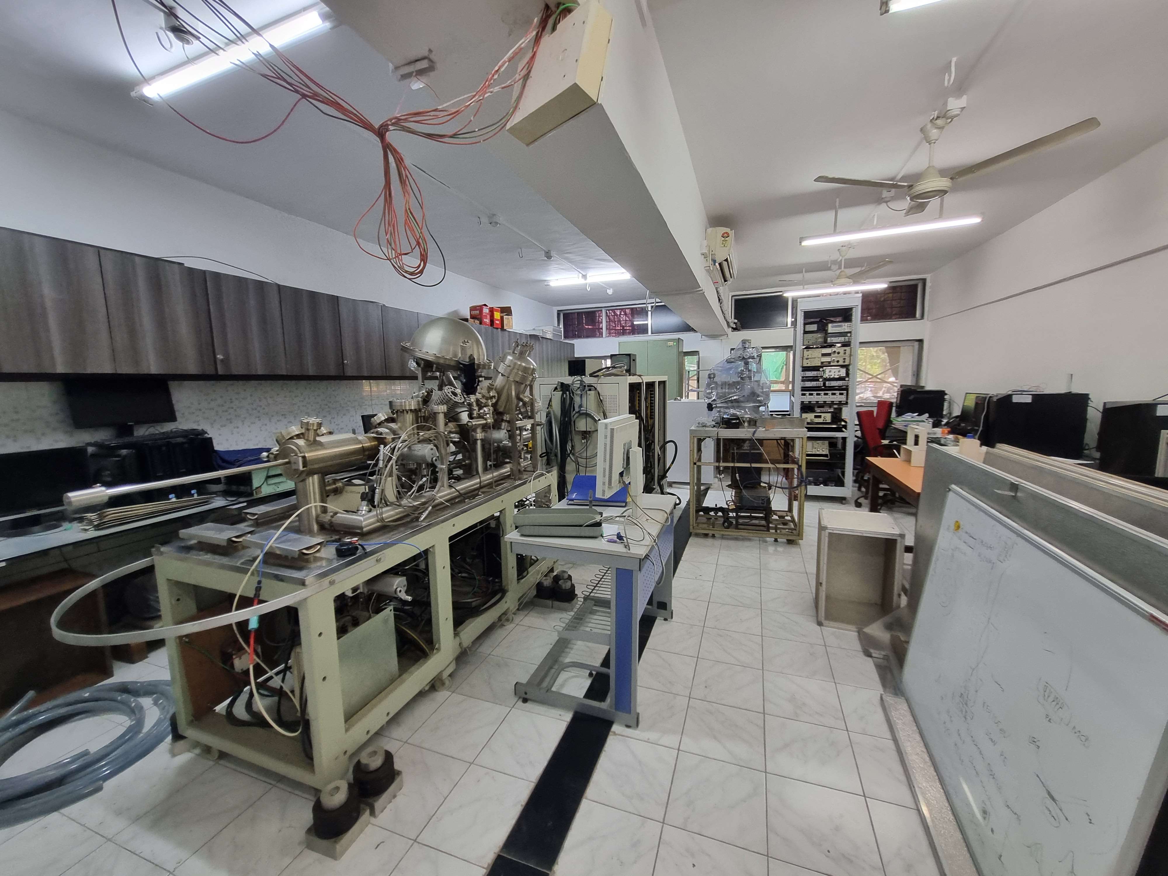
Quick view of Laboratory


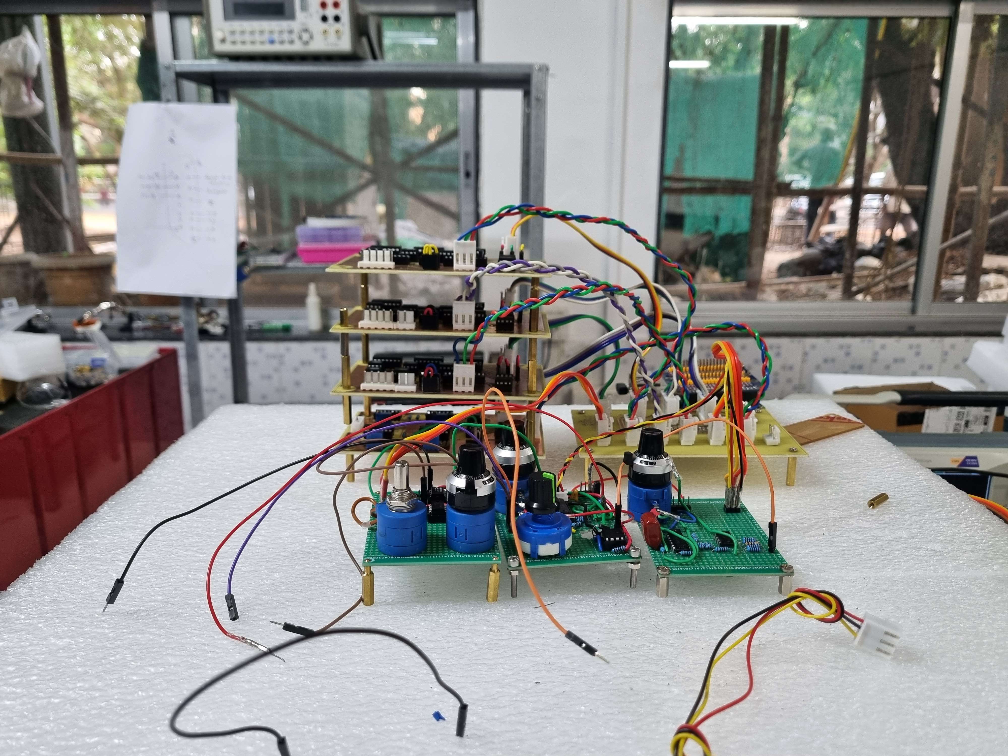
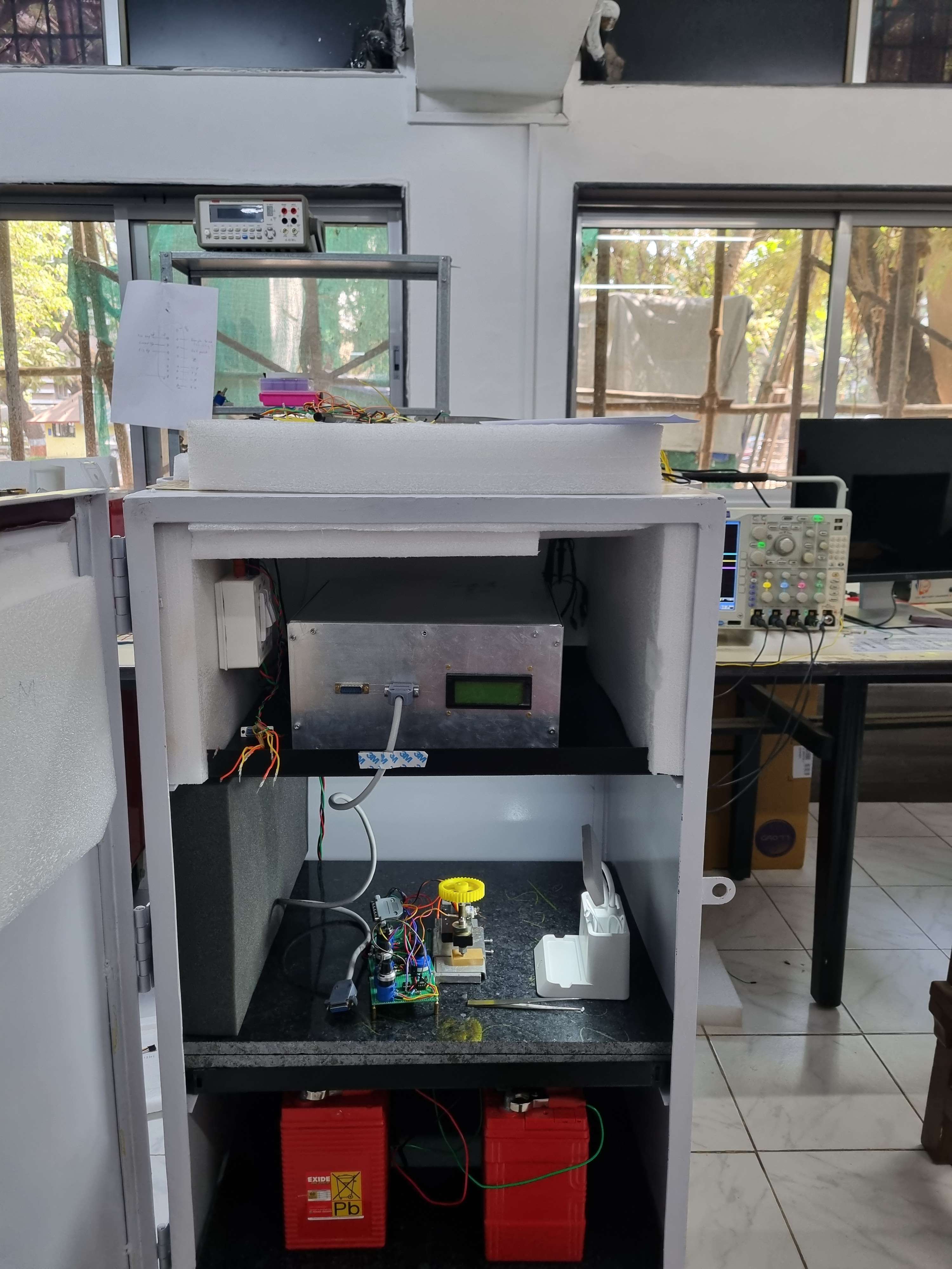
Home made STM electronics Faraday Cage for STM Lab one month ago
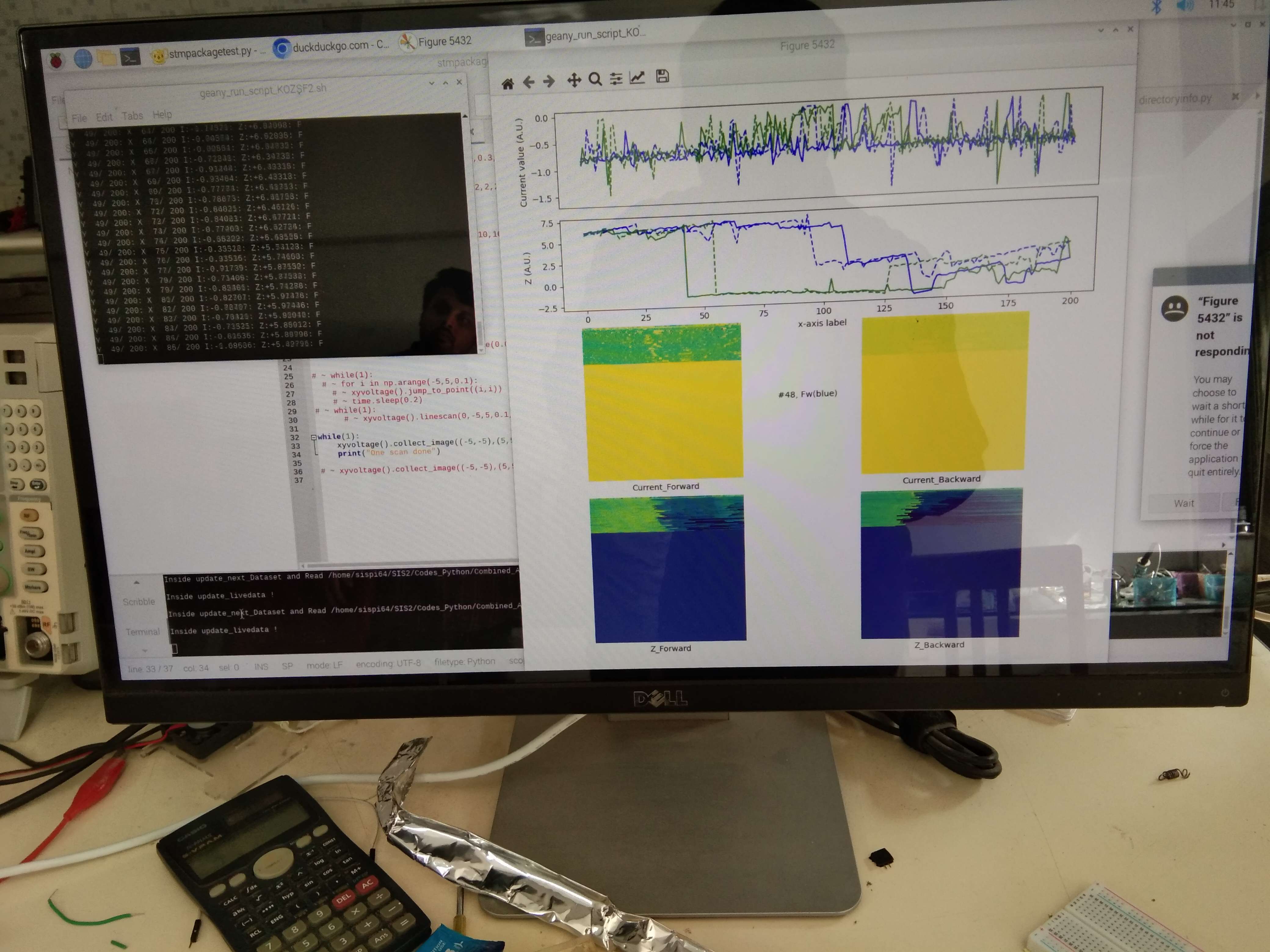
Electron Spectroscopy for Chemical Analysis Brand New Dual Polarity High Voltage Electronics Live plot STM Data collection using Python
x

About


We are setting up the state-of-the-art Ultrahigh Vacuum based Surface and Interface Science research group in IIT Bombay.

Our Interest


Group research interests are focused on (but not limited to) electronic structure studies of:

For more details feel free to contact over email or in-person.

Ongoing Projects


There are multiple choices of projects available immediately for short and long term. Proposed topics are:

Feel free to contact for more details such as currently available instrument/facility for mentioned projects and/or discuss about your interest.

Opportunities


If you have interest in developing electronic circuits, and looking for open opportunity in hands-on scientific instrument design, either full or part time, you may contact.

Looking for:

Feel free to contact me for more details or visit us in the Laboratory.

Please note that we are currently unable to provide accommodation or financial support for your stay or visit. However, if this is not a limitation for you, mention it explicitly when contacting us.

Techniques


We are currently working with our

Research Image

Members


Our members are thoughtfully chosen:

maniraj

Prof. Dr. Maniraj Mahalingam

Assistant Professor

Group leader and active team player.

PhD(12/2007-04/2014) UGC-DAE CSR, Indore, India

PDF(05/2014-07/2019) University of Kaiserslautern, Kaiserslautern, Germany

PDF(08/2019-05/2021) Martin Luther University, Halle, Germany

priyamedha

Dr. Priyamedha K. R. Sharma

Post-Doctoral Fellow

Received PhD from IIT Mandi.

Working from Dec. 2022.

shanmi

Mr. Shanmi Deibor Syntem

Ph.D. Fellow

M.Sc. from IIT Madras.

Working from Sep. 2022.

saikat

Mr. Saikat Ghoah

Summer Intern 2024

M.Sc. from IIT Bombay 2024.

Publications


STM Setup


Scanning Tunneling Microscopy is used to investigate surface morphology and atomic structure with angstrom-range accuracy and picometer-range precision in optimal cases.

Tip Making

Chemically etched tip (metal wire) in close proximity to the graphite sample, chilling in a casual ambient condition

Home made chemically etched metal tip
Home made tip holder

Electronics Design

Our Electronics are home brewed, step by step improved from the breadborad to PCB using KiCAD 3D model design.

Below are a set of 3D views showcasing an electronics board in action, navigating atom locations. We utilized the MCP4922 12-bit digital-to-analog converter and the MCP3208 8-channel analog-to-digital converter, along with a bunch of instrumentation ICs, to set up our lateral scanner electronics.

Digital to Analog Converter
Analog to Digital Converter

Breadboard DAC designed for our scanner, all under the control of a Raspberry Pi.

Upgraded PCB for the DAC, and universal board designed for a pre-amp (10^8 V/A) and PID circuit, powered by 2x 12 V batteries.

ADC with custom attenuation and bipolar to unipolar conversion unit

PID and pre-amp (of course not ideal, but does basic work)

preamp & PID controller
DAC & Raspberry pi

Data Collection

More than 15 Python modules are in sync and counting up, for counting atoms!

live plot
liveplot2

Hardware Parts

We are currently employing a stepper motor with a worm gear setup for coarse and fine approach adjustments.

Our scanning mechanism currently utilizes a piezoelectric

buzzer plate,
buzzer plate

budget-friendly piezoelectric plate that works fair enough to see atoms, as tested by many DIY hobbyist

typically used for speaker purposes. This choice is budget-friendly and provides ample room for elaborate testing.

Photoemission facility


Equipment details

The instrument consists of both monochromatized and non-monochromatized X-ray light, and ultraviolet light sources. It also includes a hemispherical electron energy analyzer for photoemission spectroscopy studies.

For surface preparation, we have Ar gas sputtering, annealing (heating), and scraping facilities.

Characterization methods

  • X-ray photoemission spectroscopy
  • Ultraviolet photoemission spectroscopy
  • Inverse photoemission spectroscopy (design and actions are under plan/progress)

Evaporation Facility

We are currently in the process of developing our own thermal evaporator suitable for:

  • Inorganic elemental metals
  • Organic molecules

If you are interested in joining us in building them, feel free to contact us.

Events


SPR-KRR workshop soon!

Prof. Jan Minar from the University of West Bohemia, Czech Republic, and our group from IIT Bombay will jointly conduct a hands-on workshop on SPR-KKR code usage in IIT Bombay. The exact date will be updated soon in the website, tentatively it is in the month of Nov-Dec 2024. Please save the website page for further updates.

If you are interested in participating as a participant, feel free to contact me.

Contact


Address: Department of Physics, Indian Institute of Technology Bombay, Powai, Mumbai- 400076, Maharashtra, India.

Email: maniraj@iitb.ac.in

Phone: [ext] 6515

Google Map

Assistant Professor

IIT Bombay

My Profile

You didn't come this far to only come this far !

Powered by w3.css